A current sensor’s datasheet bandwidth describes how fast it can see a transient. It says very little about how fast a system built around that sensor can act on one — and for any protection or safety function with a hard time budget, that second number is the one that matters.
Once a shunt is small and accurate enough to sit inside a control loop rather than on a lab bench, its job changes. It stops being an instrument that records a waveform for later analysis, and becomes a component whose output has to cross a threshold and trigger a reaction — a short-circuit trip, a breaker, a safety stop — before the fault has done damage. In that role, three delays stack up between the current event and the reaction: the sensor’s own transfer behaviour, whatever filtering is needed to make the signal usable, and the threshold margin that has to be added if the signal is not trustworthy close to that threshold.
That third term is easy to overlook. A sensor whose transfer function rings or deviates by tens of percent inside its own bandwidth forces the trip threshold to sit further away from the real fault level, and often needs a blanking window on top, simply to avoid false trips on ordinary switching transients. Fidelity and reaction time are not competing goals here — fidelity is what buys the margin back.
Bandwidth on paper vs. bandwidth that acts
This is also why the 3 dB figure on a shunt’s datasheet is a limited guide. It is normally derived from a vector network analyser measurement, and a VNA excites a shunt differently from how it operates in a power circuit: both the load path and the measurement path are forced into one closed loop, so parasitics that belong exclusively to the load path show up in the measured response even though they don’t limit what the measurement path can actually resolve.
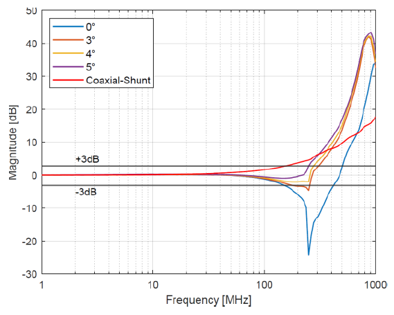
We demonstrated this directly by mechanically shortening a commercial coaxial shunt’s outer lead — a change confined entirely to the load path — and watched the measured transmission flip from inductive to capacitive behaviour, despite the internal coupling geometry being untouched. The datasheet number moved; the sensor’s real measurement mechanism did not. What a fault-detection circuit needs validated is the time-domain response, not the VNA curve.
(Full methodology: H. Lutzen, J. Müller, V. Polezhaev, T. Huesgen and N. Kaminski, “From Insight into Bandwidth to Fast-Transient Precision: Diamond M-Shunts for Wideband Current Measurement,” CIPS 2026, Dresden, Germany.)
Coupling strength is a design knob, not a parasitic
The Diamond-M-Shunt’s rhombic split-coupling geometry makes the electromagnetic coupling between load and measurement path an explicit, adjustable parameter — set by the widening angle of the traces. We built and measured variants from 0° to 5°. A 4° angle gave the highest nominal 3 dB bandwidth; a 5° angle gave the lowest in-band deviation, holding within ±10 %, and visibly cleaner double-pulse waveforms. For measurement work, 5° is the right answer — the higher bandwidth number at 4° comes with distortion that a VNA curve alone won’t show.
That trade-off is worth pushing further as a thought experiment. If a circuit only needs to know that di/dt has crossed a limit — not reconstruct the waveform — then over-coupling beyond the 5° compensation point stops being a defect. It emphasises exactly the fast components an edge detector cares about, at the cost of amplitude accuracy nobody in that role needs. We have not characterised an over-coupled geometry for detection latency specifically, and it would need its own figures of merit rather than a 3 dB number. But it illustrates the underlying point: coupling strength should be chosen for what the output is used for — plotted, or acted on — and today almost no shunt is designed with the second case in mind.
Small enough to sit at the fault
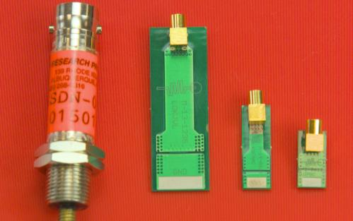
None of this helps if the sensor can’t physically be where the fault happens. The Mini-M-Shunt line closes that gap: bandwidths beyond 300 MHz and residual insertion inductance below 1 nH in 6 × 12 mm and 6 × 18 mm devices on standard SMD footprints, with continuous current capability of 7–10 A and pulse tolerance above 1 kA. Their surface-to-volume ratio also means the usual adiabatic datasheet estimate is conservative — thermal coupling to the PCB and vias sustains meaningfully higher currents in practice.
The practical consequence is placement. A Mini-M-Shunt fits directly into a critical current path, a Kelvin-source path, or inside a power module — measuring the current of one device rather than the aggregate at the DC link. That matters because fault signatures that are obvious at the device are frequently invisible further out: our Kelvin-source measurements on bond wire lift-off show dynamic current asymmetries at the individual switch that a load-current measurement alone would miss.
(Full methodology: H. Lutzen, J. Müller, V. Polezhaev, S. Clausner, T. Huesgen and N. Kaminski, “Pushing Miniaturisation in Current Sensing: Ultra-Compact Mini-M-Shunts for Even Faster Transients,” PCIM Europe 2026, Nuremberg, Germany.)
Where the budget still has room
Any system with a hard reaction-time budget — short-circuit protection in SiC/GaN converters, solid-state breakers, battery disconnect, or the drive-side safety functions that set the allowed operating envelope in motion control — inherits a detection term inside that budget. The mechanical and control contributions have mostly been optimised for years. Detection latency has largely been treated as a fixed cost of the sensor you happen to have. We don’t think it has to be.
Related publications
