Author: Hauke Lutzen

  • Detecting Bond Wire Lift-Off with Machine Learning – Using the M-Shunt Kelvin-Source Current

    Can a healthy chip be told apart from a degraded one just by feeding its switching waveform into a neural network? A new collaboration between Kyushu University and IALB shows that it can — and that the Kelvin-source current is the one input the network can trust even when temperature gets in the way.

    Bond wire lift-off is one of the classic wear-out mechanisms in power modules: as wires fatigue and detach, the source resistance and inductance of the affected chip rise, current sharing between parallel devices shifts, and the switching waveform changes shape. Machine-learning classifiers trained on such waveforms have already shown promise for detecting lift-off without any dedicated monitoring circuit — but almost always for a single chip. Real power modules, however, are built from several chips in parallel, and it was unclear whether the same approach would still work once device-to-device mismatch and temperature differences start shaping the waveform as well.

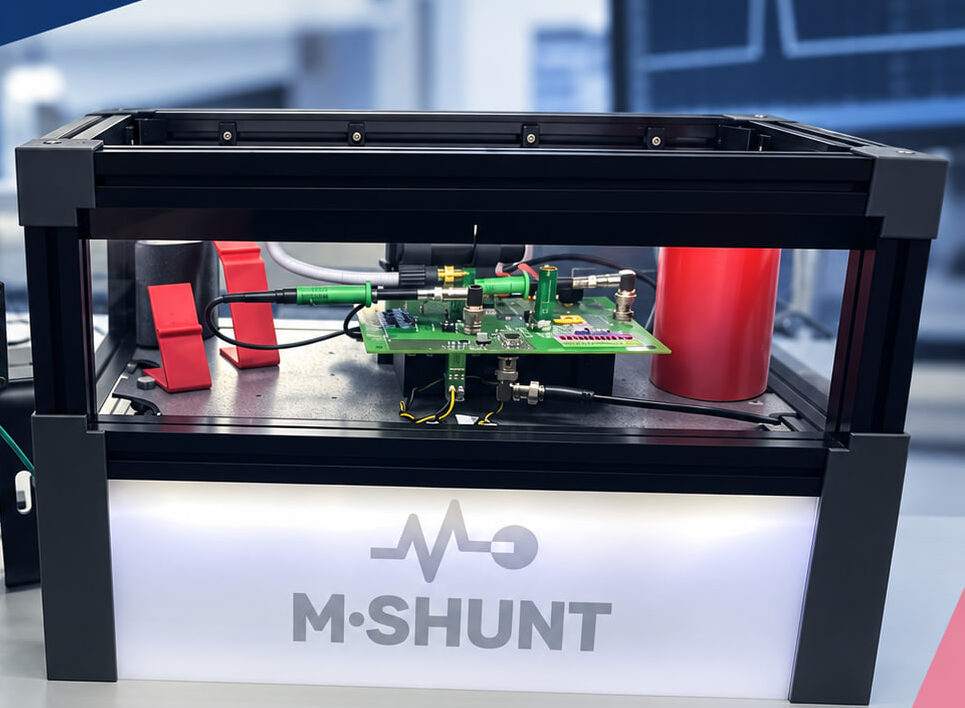
    The study addresses exactly that. Two discrete SiC-MOSFETs were connected in parallel and put through double-pulse tests, with the M-Shunt measuring the load current and a Mini-M-Shunt measuring the Kelvin-source current. Source bond wires were then cut in a controlled sequence — from all four intact down to just one remaining — to simulate four stages of degradation, from healthy to heavily damaged. A convolutional neural network was trained to classify the degradation stage from the switching waveform, and the experiment was repeated across three current-balance conditions, obtained by pairing devices with different threshold voltages.

    The gate voltage and the Kelvin-source current turned out to be the most dependable inputs, both reaching close to 100 % classification accuracy regardless of current imbalance or which of the two devices was evaluated. The drain-source voltage and load current, by contrast, were far less consistent — drain-source voltage accuracy collapsed to around 25–30 % during turn-off, and load-current accuracy dropped to about 52 % for one device during turn-on, simply because degradation left too faint a mark on those particular waveform segments.

    The more demanding test came next: could rising temperature alone — with no wires cut at all — fool the network into reporting degradation? For the gate voltage during turn-on, the answer was yes: its ringing amplitude fades with temperature in much the same way it fades with wire lift-off, and the classifier’s healthy-state accuracy dropped to almost 0 % once the device was heated. The Kelvin-source current showed no such confusion. Across every temperature step tested, it kept a healthy-state classification rate of around 99–100 %, correctly recognising an undamaged device as undamaged even as its temperature rise by close to 60 °C.

    That combination — high sensitivity to genuine degradation and near-total immunity to temperature-driven false alarms — is what makes the Kelvin-source current a particularly promising basis for machine-learning-based condition monitoring in parallel-chip power modules, without adding dedicated sensing hardware beyond the M-Shunt itself.

    Related publications
  • When Heat Looks Like Damage: Separating Temperature and Degradation Effects with the M-Shunt

    Bond wire lift-off and rising junction temperature both disturb the current sharing of parallel-connected SiC-MOSFETs — and in steady state, they can look surprisingly alike. Telling them apart matters: mistaking a harmless temperature swing for degradation (or the other way round) undermines any real-time health monitoring scheme built on the Kelvin-source current.

    A new study by researchers from the University of Bremen and Kyushu University, to be presented at ICSCRM 2026 in Yokohama, investigates exactly this ambiguity — and shows how to resolve it.

    Parallel SiC-MOSFETs are the standard way to scale up the current-carrying capability of a power module. But unavoidable mismatches between chips, together with layout-driven differences in parasitic inductance, mean the current is rarely shared perfectly. The Kelvin-source (KS) current — the small balancing current that flows through the shared source connection of two paralleled devices — has already been shown to reveal such asymmetries, including the very first stages of bond wire lift-off, well before they show up in the load current. The open question this work addresses is how a second disturbance, junction temperature, interacts with that same signal.

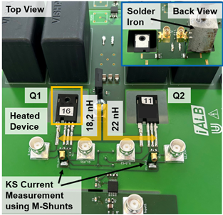
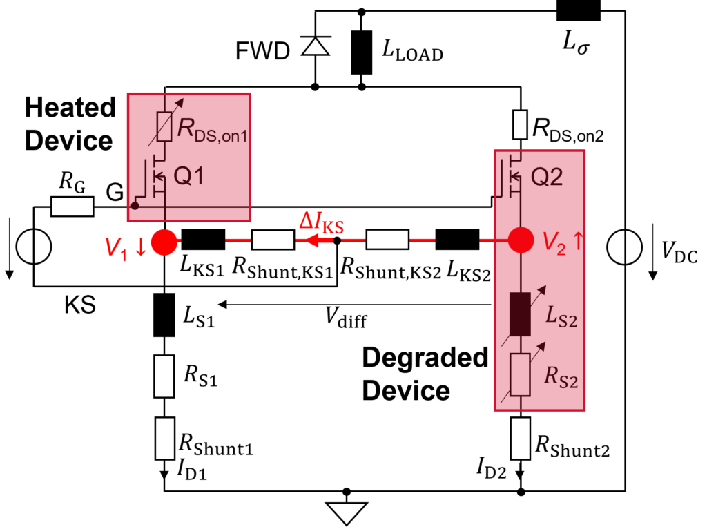
    Using two SiC-MOSFETs in TO-247-4L packages, one device was deliberately heated with a soldering iron mounted to its backplate while the KS current was captured with M-Shunts placed in both the load and the KS path. As the heated device’s junction temperature rises, its threshold voltage drops while its on-state resistance increases — two effects that pull the balancing current in opposite directions during a single switching event. The result is a distinctive transient signature: the KS current first swings towards one polarity as the lower threshold voltage lets the heated device turn on earlier, then reverses towards the opposite polarity as its higher on-state resistance takes over in steady state.

    Bond wire lift-off behaves quite differently. Removing bond wires increases both the source resistance and inductance of a device, which simply shifts the KS current waveform in one direction, in both the transient and steady-state phases, without the reversal seen for temperature. While the steady-state values for both effects can end up looking similar, the transient shape does not — the opposite-direction peak is a reliable fingerprint of a temperature disturbance rather than genuine degradation.

    The findings point to the transient KS current, not just its steady-state value, as the more robust basis for real-time health monitoring — and the authors suggest that an AI-based evaluation of the signal is a promising next step towards distinguishing the two effects reliably in the field.

    Related publication The underlying research will be presented at ICSCRM 2026, Yokohama, Japan (27 September – 2 October 2026).

  • Detecting Bond Wire Lift-Off in Parallel SiC-MOSFETs — with the M-Shunt Kelvin-Source Current

    Bond wire lift-off is one of the classic degradation mechanisms in power semiconductor packages, driven by thermomechanical stress from repeated load cycling. As wires detach from the chip’s source metallisation, the parasitic source inductance and resistance increase — with direct consequences for switching behaviour, and, in parallel-connected devices, for how the current is shared between chips.

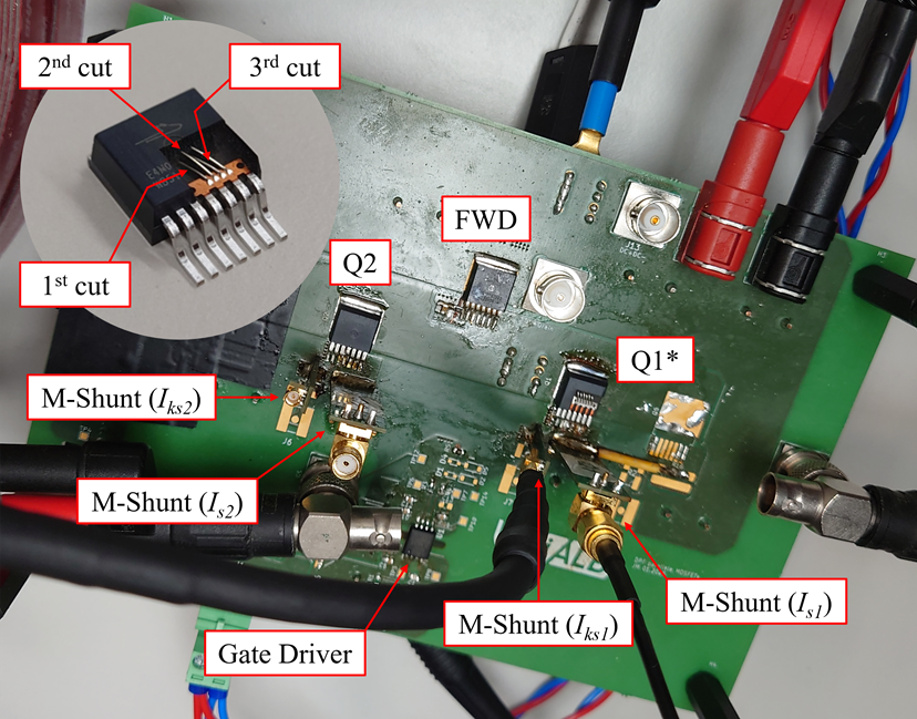
    A study presented at ISPS 2025 by researchers from the University of Bremen, METU and Kyushu University investigates this effect on discrete TO-263 packaged SiC-MOSFETs, using the M-Shunt to capture both the load current and, for the first time in this setup, the Kelvin-source (KS) current.

    For a single device, removing bond wires one by one — simulating progressive lift-off — increases the source inductance and resistance, confirmed by Ansys Q3D and LTspice modelling of the package. The measured effect is consistent: the rate of change of current and voltage during turn-on drops, and the switch takes measurably longer to turn on, with total switching losses rising as more wires are removed.

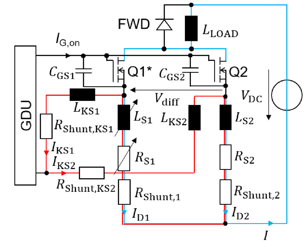
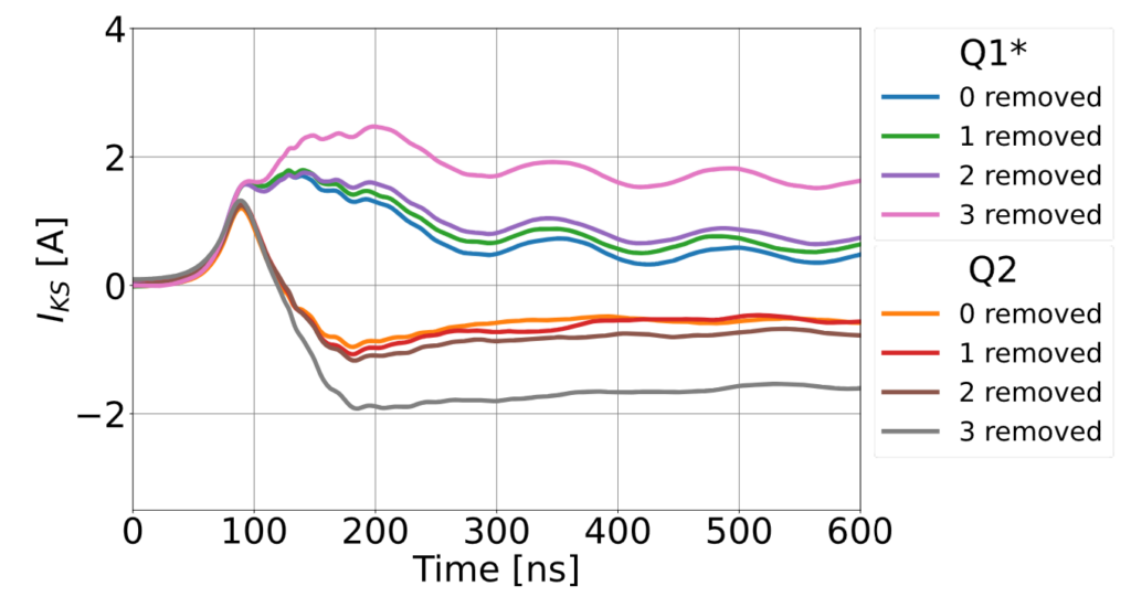
    In two parallel-connected devices, the same effect shows up as a current imbalance. As bond wires are progressively removed from one of two paralleled MOSFETs (Q1*), that device’s current slows down and shifts to its unaffected neighbour (Q2) — which then has to carry more current and absorbs the additional switching losses. This drain-current imbalance is measurable, but at low numbers of removed bond wires it is initially masked by ordinary chip-to-chip tolerances, so it only becomes a reliable indicator once enough bond wires are gone.

    The Kelvin-source current is more sensitive. Because the KS path is decoupled from the load loop but shared between both devices, any difference in source impedance between the two chips drives a measurable current through this shared connection — increasing systematically with every bond wire removed, and clearly identifiable from the very first removed wire, regardless of which position on the chip it is removed from.

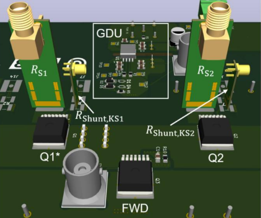
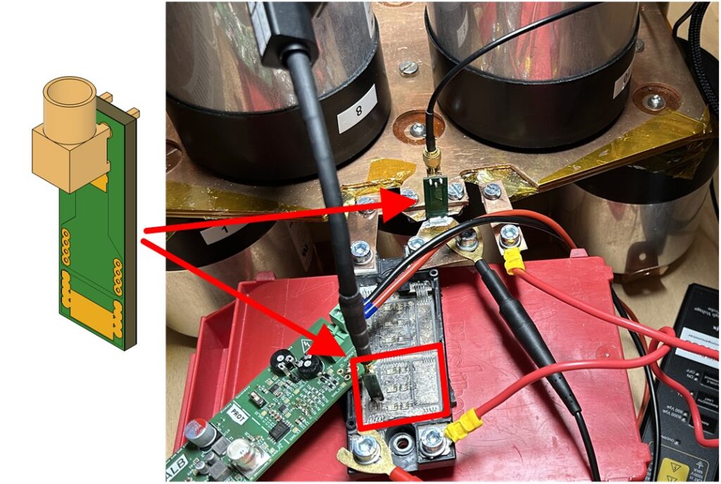
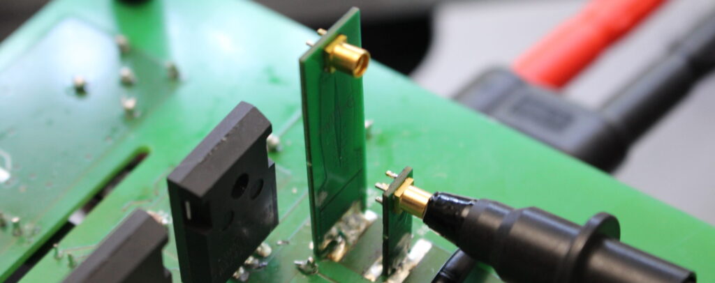
    To resolve this, the PCB carries four M-Shunts: two in the load path, capturing the individual drain currents of Q1* and Q2, and two more, dedicated units in the Kelvin-source path. The low self-inductance and compact footprint of the M-Shunt make it possible to integrate all four sensors into a PCB layout designed for symmetric, low-inductive switching — without the shunts themselves distorting the fast transients they are meant to measure.

    The results point towards Kelvin-source current monitoring as a practical building block for health monitoring of power semiconductors — a clean, low-effort signal that can flag the very first bond wire lift-off well before it is visible in standard drain-current or voltage measurements.

    Related publication The underlying research was published at ISPS 2025.

  • Detecting Current Asymmetries in Multi-Chip SiC Power Modules — with the M-Shunt

    Multi-chip power modules pack several SiC chips in parallel to handle higher currents. In an ideal world, each chip carries its fair share of the load. In practice, small differences in chip parameters or bonding wire connections can cause uneven current distribution — with consequences for reliability and safe operating area.

    Detecting these asymmetries is not straightforward. Standard measurements like drain-source voltage, gate-source voltage, or total load current show little to no change even when current distribution is significantly uneven. A different approach is needed.

    In a study presented at ISPSD 2026, researchers from the University of Bremen and Kyushu University show that the Kelvin Source (KS) path offers exactly that. In a three-chip SiC half-bridge module, the KS current of individual chips responds measurably to changes in source impedance — even when the total load current looks perfectly normal. As bonding wires are progressively removed from one chip, the KS current shifts detectably while the standard measurement signals remain essentially flat. The method works down to complete chip failure — at which point the module was still functional, but the remaining chips were operating under increased stress.

    Fig. 1: Detecting current asymmetries in multi-chip SiC power modules using the Kelvin source path.

    Two types of M-Shunts were central to the measurement setup: one for load current detection, and a second placed in the KS path as a dedicated current sensor. The combination enabled to resolve the small, fast transient signals in the KS path alongside the main switching waveforms — a measurement challenge that conventional current probes would struggle with given the bandwidth and footprint requirements.

    The results suggest a viable route to detecting design issues during development as well as degradation during operation — without requiring access to individual chip terminals beyond the KS path.

    Related publication
    The underlying research was published at ISPSD 2026.

    Fullpaper link: ISPSD 2026

  • What is the M-Shunt — and why does it matter for power electronics?

    Measuring current sounds straightforward. In practice, doing it accurately in fast-switching power electronics is one of the more demanding measurement challenges around — and the M-Shunt was developed specifically to meet it.

    The problem with fast switching

    Modern power semiconductors based on SiC and GaN switch in nanoseconds. That speed is what makes them efficient — but it also means that current can change by hundreds of amperes within a few nanoseconds. To capture that faithfully, a current sensor needs high bandwidth, low parasitic inductance, and enough physical compactness to fit into a switching circuit without disturbing it.

    Conventional shunt resistors work well at lower speeds but run into trouble here. Their parasitic inductance introduces measurement errors precisely when the current is changing fastest. Rogowski coils and Hall-effect sensors have their own bandwidth and integration challenges. None of them combine high bandwidth, low inductance, and small footprint cleanly.

    The coaxial principle

    The M-Shunt is based on the coaxial shunt resistor concept — a design in which the measurement path runs through the centre of a cylindrical current-carrying conductor. By Ampere’s law, the magnetic field inside such a conductor is shielded from external fields, which means the measurement loop sees only the voltage drop across the resistor and not the electromagnetic interference from the switching circuit around it. The result is high EMI stability alongside high measurement bandwidth.

    What makes the M-Shunt distinctive is how this principle is implemented on a PCB. The design, developed at the University of Bremen, integrates the coaxial structure into a compact, surface-mountable form factor — small enough to fit directly into a power module or test setup without adding significant parasitic inductance to the current path.

    Fig. 1: Key properties of the M-Shunt.

    What it enables

    The combination of properties — high bandwidth, low insertion inductance, high current capability, and EMI stability — makes the M-Shunt suitable for measurement tasks that other sensors struggle with: Double Pulse Tests on SiC and GaN devices, current sensing inside power modules, and applications where the sensor must sit directly in the switching loop without compromising its behaviour.

    It also opens up measurement paths that were previously impractical, such as placing a sensor in the Kelvin Source path of a multi-chip module to detect current asymmetries between parallel chips — something conventional probes cannot do at the required bandwidth and footprint.

    More details on how the M-Shunt is applied in practice can be found in our application notes and published papers.

  • Booth 6-410 – ECPE/Eurocomp: Open Module with embedded M-Shunt

    Booth 6-410 – ECPE/Eurocomp: Open Module with embedded M-Shunt

    In Hall 6, Booth 6-410, we present open-frame power modules with embedded M-Shunts soldered directly into the circuit.

    The unsealed, open-housing design gives a clear view of the M-Shunt integration and illustrates our Kelvin Source measurement approach in a real module environment. This demonstration highlights how the M-Shunt enables precise, low-inductance current sensing without compromising the switching performance of the module.

    For a detailed explanation of the underlying measurement principle, visit the Kelvin Source technology page on our website.

  • Booth 6-419 – Uni Bremen / IB-Billmann: Insights & Test-as-a-Service

    Booth 6-419 – Uni Bremen / IB-Billmann: Insights & Test-as-a-Service

    In Hall 6, Booth 6-419, we share a joint booth with the University of Bremen’s HiPE-Lab and IB-Billmann — our home booth at PCIM 2026.

    Stop by for a conversation about the latest M-Shunt developments, current measurement challenges, or anything power electronics. We are happy to discuss your specific application and explore whether and how the M-Shunt fits your measurement needs.

    Our partners from HiPE-Lab present their capabilities for design, simulation, and testing of power electronic systems under realistic environmental and electrical conditions — covering the full range from early-stage development through to system-level validation.

  • Booth 7-157 – PMK / Iwatsu / Cleverscope: Full Scale Module Pulse Tester with Parallel Devices

    Booth 7-157 – PMK / Iwatsu / Cleverscope: Full Scale Module Pulse Tester with Parallel Devices

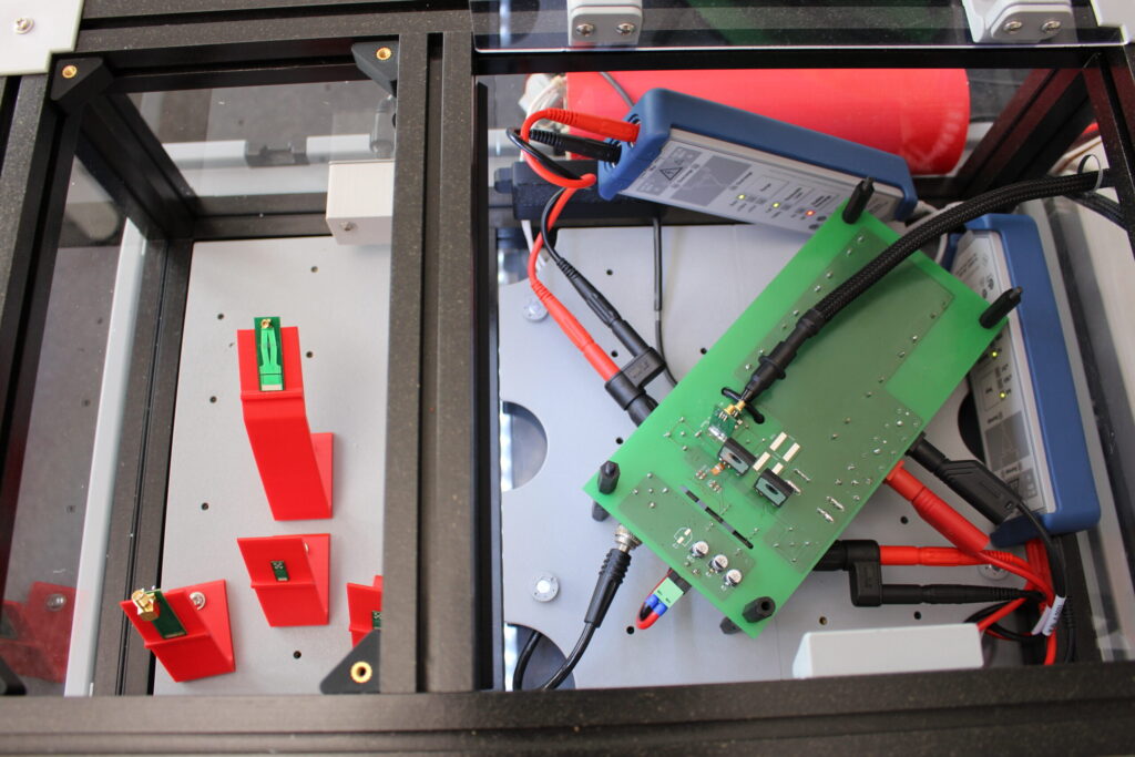
    In Hall 7, Booth 157, we present a double pulse test setup with M-Shunts integrated into the load path of a module measurement.

    The system is measured using the FireFly probe from PMK Mess- und Kommunikationstechnik GmbH and controlled via a Cleverscope oscilloscope, which also provides an optically isolated input stage.

    This setup demonstrates high-bandwidth current measurement under realistic switching conditions

  • Booth 7-100 – Rohde & Schwarz: SiC Double Pulse Test Setup

    Booth 7-100 – Rohde & Schwarz: SiC Double Pulse Test Setup

    In Hall 7, Booth 7-100, we demonstrate a double pulse test of discrete SiC MOSFETs in a dedicated setup at the Rohde & Schwarz booth.

    The Mini M-Shunt and Diamond M-Shunt are used side by side to compare measurement performance under fast transient switching conditions — giving a direct, practical impression of how shunt geometry affects bandwidth and signal quality.

    This setup builds on our ongoing collaboration with Rohde & Schwarz. In May 2026, Hauke Lutzen joined their Power Electronics Online Conference as an invited speaker — presenting insights into high-bandwidth current measurement and advanced sensor technologies for fast-switching applications. Read the full recap on our website.

    Open Video