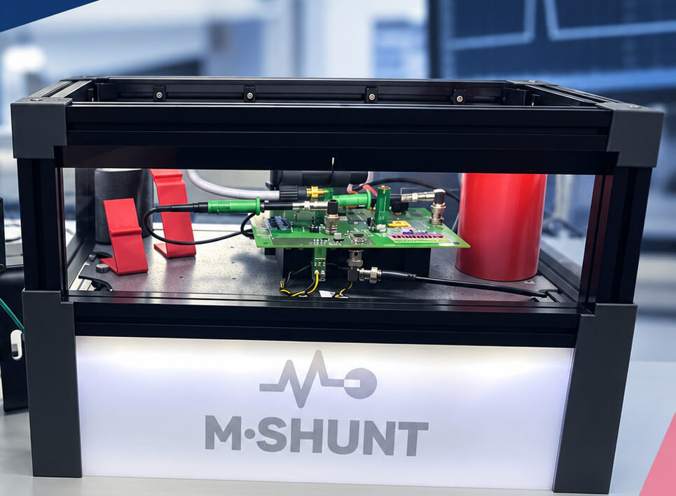
Bond wire lift-off is one of the classic degradation mechanisms in power semiconductor packages, driven by thermomechanical stress from repeated load cycling. As wires detach from the chip’s source metallisation, the parasitic source inductance and resistance increase — with direct consequences for switching behaviour, and, in parallel-connected devices, for how the current is shared between chips.
A study presented at ISPS 2025 by researchers from the University of Bremen, METU and Kyushu University investigates this effect on discrete TO-263 packaged SiC-MOSFETs, using the M-Shunt to capture both the load current and, for the first time in this setup, the Kelvin-source (KS) current.
For a single device, removing bond wires one by one — simulating progressive lift-off — increases the source inductance and resistance, confirmed by Ansys Q3D and LTspice modelling of the package. The measured effect is consistent: the rate of change of current and voltage during turn-on drops, and the switch takes measurably longer to turn on, with total switching losses rising as more wires are removed.
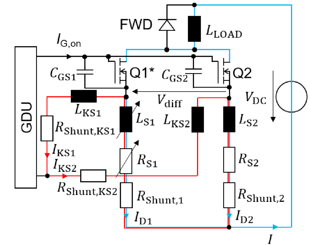
In two parallel-connected devices, the same effect shows up as a current imbalance. As bond wires are progressively removed from one of two paralleled MOSFETs (Q1*), that device’s current slows down and shifts to its unaffected neighbour (Q2) — which then has to carry more current and absorbs the additional switching losses. This drain-current imbalance is measurable, but at low numbers of removed bond wires it is initially masked by ordinary chip-to-chip tolerances, so it only becomes a reliable indicator once enough bond wires are gone.
The Kelvin-source current is more sensitive. Because the KS path is decoupled from the load loop but shared between both devices, any difference in source impedance between the two chips drives a measurable current through this shared connection — increasing systematically with every bond wire removed, and clearly identifiable from the very first removed wire, regardless of which position on the chip it is removed from.
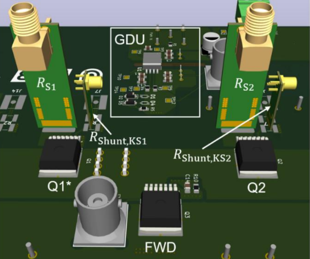
To resolve this, the PCB carries four M-Shunts: two in the load path, capturing the individual drain currents of Q1* and Q2, and two more, dedicated units in the Kelvin-source path. The low self-inductance and compact footprint of the M-Shunt make it possible to integrate all four sensors into a PCB layout designed for symmetric, low-inductive switching — without the shunts themselves distorting the fast transients they are meant to measure.
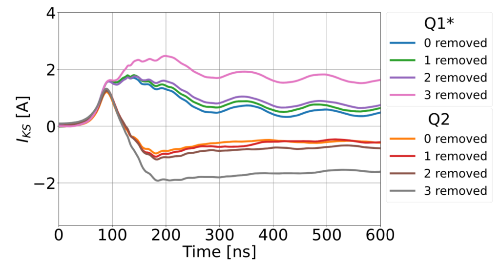
The results point towards Kelvin-source current monitoring as a practical building block for health monitoring of power semiconductors — a clean, low-effort signal that can flag the very first bond wire lift-off well before it is visible in standard drain-current or voltage measurements.
Related publication The underlying research was published at ISPS 2025.